- 您现在的位置:买卖IC网 > Sheet目录279 > 101-1147 (Rabbit Semiconductor)KIT RIO PROGRAM I/O
�� �
�
�Hardware� Connections�
�/CS�
�PDN�
�/IORD� nc�
�nc�
�OUT�
�/IOWR� /CORE� PA0� D0�
�PA0�
�VBAT�
�PA2� PA3�
�D3�
�PA6�
�PA5�
�PB0�
�PA7�
�PB2� PB2�
�P_� I�
�PB6�
�PB5�
�G� _� C�
�PB7�
�PC6�
�PC5�
�PC2�
�SERI�
�nc�
�SERI�
�PE4�
�PE3�
�PE6�
�PE5�
�PD0� PC0�
�SERI�
�SERI�
�nc�
�PD2�
�PD1�
�PD4�
�PD3�
�SER� +3.3� V�
�PDN�
�S5�
�S4�
�S3�
�1.� Prepare� the� Prototyping� Board� for�
�Development�
�Snap� in� four� of� the� plastic� standoffs� supplied� in� the� bag�
�of� accessory� parts� from� the� RIO� Programmable� I/O� Kit�
�in� the� holes� at� the� corners� as� shown.�
�TP2�
�GND�
�1�
�S1�
�RESET�
�R4�
�C24�
�R3�
�J2�
�R16�
�Q7�
�CORE�
�PE7�
�DS4�
�J1�
�R1�
�U1�
�D1�
�C6�
�PE7�
�RCM1� C26�
�C25� /CORE�
�PB1�
�PD5� PD6�
�PD7� CONV� SERB�
�VREF� GND� PC4� SERI�
�J11� nc� SERI� PU� PU� PU�
�PC5� SERO� P/� /� I� CA0� G/� /� C�
�PB0� SCLK� PDN� PDN� PDN�
�+3.3� V� GND�
�RST�
�RESET�
�PA1�
�PA3� PA4� PA4� D4�
�PB7� PC0�
�PC1� PC2� PE4� WAIT�
�PC3� PC4� J7� Y1�
�SERC�
�PC7� PE0�
�PE1� PE2� PC3� SERO�
�PD2� SCLK�
�J12� R6�
�SERD�
�PC1� SERO�
�PC3� SCLK�
�J15�
�J16� J8�
�C1� C2�
�HOT� U2�
�PA5� D5�
�PA6� D6�
�PA7� D7�
�PB3� PB4� PB3� CA0�
�PB4� CA1�
�PB5� CA2�
�C3�
�R5�
�PE1� /CS�
�PA1� D1�
�PA2� D2�
�C28�
�C8�
�C7�
�/RD� /WR�
�C10�
�J9� +5� V�
�BT1�
�C15�
�J17�
�J14�
�RP1�
�J4� J6�
�C14�
�C18� C17�
�C19� C16�
�GND�
�U3�
�C12�
�C11�
�PU�
�/PAR�
�GND�
�C0P3�
�R15� C33�
�1�
�GND�
�C0P2�
�R14� C32�
�1�
�RX12�
�+5� V�
�GND�
�+3.3� V�
�C0P1�
�R13� C31�
�1�
�RX13� RX15�
�RX14� RX16�
�RX11�
�RX11�
�RX19�
�+3.3� V�
�GND�
�+5� V�
�C0P0�
�R12� C30�
�1�
�S2�
�RX17�
�RX18�
�RX1�
�RX2�
�RX3�
�RX4�
�TP1�
�+3.3� V�
�GND�
�GND�
�RX41�
�RX42�
�CX1�
�CX2�
�+3.3� V�
�UX25�
�UX3�
�+5� V�
�GND�
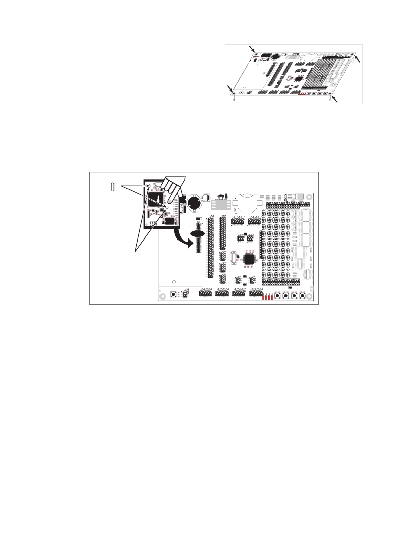
�2.� Attach� Module� to� Prototyping� Board�
�Turn� the� RCM4110� module� so� that� the� mounting� holes�
�Figure� 1.� Insert� Plastic� Standoffs�
�of� the� RCM4110� line� up� with� the� corresponding� holes�
�on� the� Prototyping� Board.� Insert� the� metal� standoffs� as� shown� in� Figure� 2,� secure� them� from� the� bottom� of�
�the� Prototyping� Board� using� the� 4-40� ×� 3/16� screws,� then� insert� the� module’s� header� J3� on� the� bottom� side�
�into� header� socket� RCM1� on� the� Prototyping� Board.�
�R13�
�R12�
�R1�
�C15�
�C6�
�RCM1�
�PDN�
�/CORE� PA0�
�PA0�
�PA3�
�PB0�
�Insertstandoffs�
�between�
�mounting� holes� and�
�Prototyping� Board.�
�RCM4110�
�C30�
�C31�
�C36�
�C38�
�C39�
�C29�
�C25� C19�
�C26� C20�
�C27� R18�
�C28R21� R19�
�R22�
�R16�
�Q7�
�C21�
�RP1�
�C23�
�R17� R16�
�C16�
�C17�
�C6�
�C7�
�U1�
�DS4�
�J1�
�R11� R9�
�R10�
�U1�
�D1�
�R3�
�JP1�
�JP2�
�JP9�
�JP6�
�JP7�
�JP3�
�JP5�
�JP4�
�C1�
�C2�
�C4�
�C26�
�C25�
�RCM1�
�+3.3� V�
�/CORE�
�RST�
�OUT�
�/IOWR�
�VBAT�
�PA1�
�PA3�
�PA5�
�PA7�
�PB1�
�PB3�
�C1� C2�
�C3�
�HOT� U2�
�PE1�
�GND�
�/IORD� nc�
�RESET�
�PA1�
�PA2�
�PA2�
�PA4� PA4�
�PA6� PA5�
�PA6�
�PA7�
�PB2� PB2�
�PB4� PB3�
�R5�
�/CS�
�/CS�
�nc�
�D0�
�D1�
�D2�
�D3�
�D4�
�D5�
�D6�
�D7�
�P_I�
�CA0�
�BT1�
�C15�
�J4�
�J17�
�J14�
�RP1�
�J6�
�RX12�
�GND�
�RX13�
�RX14�
�+5� V�
�GND�
�+3.3� V�
�RX15�
�RX16�
�RX17�
�RX18�
�RX41�
�RX42�
�CX1�
�RX1�
�RX2�
�RX3�
�CX2�
�UX25�
�+3.3� V� UX3�
�+5� V�
�GND�
�PB7�
�PB5�
�PB7�
�PB6� PB4�
�PB5�
�PC0�
�CA1�
�CA2�
�G_C�
�/RD�
�/WR�
�RX4�
�nc�
�Line� up� mounting�
�holes� with� holes�
�on� Prototyping� Board.�
�PC1�
�PC3�
�PC5�
�PC7�
�PE1�
�PE3�
�PE5�
�PE7�
�PD1�
�PD3�
�PD5�
�PD7�
�PC2� PE4�
�PC4�
�PC6�
�PC2�
�PE0�
�PE2� PC3�
�PE4� PD2�
�PE6�
�PD0� PC0�
�PD2� nc�
�PD4� PC1�
�PC3�
�PD6�
�CONV�
�J7�
�SERC�
�J12�
�SERD�
�J15�
�SERB�
�WAIT�
�SERI�
�SERI�
�SERO�
�SCLK�
�SERI�
�SERI�
�SERO�
�SCLK�
�Y1�
�C28�
�R6�
�C18�
�C19�
�C8�
�C7�
�C10�
�C14�
�C17�
�C16�
�U3�
�C12�
�C11�
�GND�
�RX11�
�RX11�
�RX19�
�VREF�
�GND� PC4�
�SERI�
�PDN�
�TP2�
�GND�
�1�
�RESET�
�R4�
�C24�
�CORE�
�J11�
�nc�
�PC5�
�PB0�
�J16�
�SERI�
�SERO�
�SCLK�
�PU�
�P/� /� I�
�PDN�
�J8�
�PU�
�CA0�
�PDN�
�PU�
�G/� /� C�
�PDN�
�J9�
�PU�
�SER� +3.3� V�
�/PAR�
�GND�
�+5� V�
�C0P3�
�R15� C33�
�C0P2�
�R14� C32�
�C0P1�
�R13� C31�
�+3.3� V�
�GND�
�+5� V�
�C0P0�
�R12� C30�
�TP1�
�+3.3� V�
�GND�
�GND�
�R3�
�PE7�
�S1�
�J2�
�S5�
�1�
�S4�
�1�
�S3�
�1�
�S2�
�1�
�Figure� 2.� Install� the� RCM4110� Module� on� the� Prototyping� Board�
�NOTE:� It� is� important� that� you� line� up� the� pins� on� header� J3� of� the� RCM4110� module� exactly� with�
�socket� RCM1� on� the� Prototyping� Board.� The� header� pins� may� become� bent� or� damaged� if� the� pin�
�alignment� is� offset,� and� the� module� will� not� work.� Permanent� electrical� damage� to� the� module� may�
�also� result� if� a� misaligned� module� is� powered� up.�
�Press� the� module’s� pins� gently� into� the� Prototyping� Board� header� socket—press� down� in� the� area� above�
�the� header� pins.� For� additional� integrity,� you� may� secure� the� RCM4110� to� the� standoffs� from� the� top�
�using� the� remaining� two� 4-40� � 3/16� screws.�
�3.� Set� Jumpers�
�Jumpers� were� placed� at� the� factory� on� Prototyping� Board� headers� J2,� J7,� J8,� J9,� and� J15� as� shown� in� Figure� 3�
�to� set� up� the� Prototyping� Board� for� the� SPI� serial� mode� used� with� the� sample� programs.� Application� Note�
�AN415,� RIO� Programmable� I/O� Kit� ,� describes� other� configuration� options.�
�4.� Connect� Programming� Cable�
�The� programming� cable� connects� the� RCM4110� to� the� PC� running� Dynamic� C� to� download� programs�
�and� to� monitor� the� RCM4110� module� during� debugging.�
�Connect� the� 10-pin� connector� of� the� programming� cable� labeled� PROG� to� header� J1� on� the� RCM4110�
�as� shown� in� Figure� 3.� Be� sure� to� orient� the� marked� (usually� red)� edge� of� the� cable� towards� pin� 1� of� the�
�connector.� (Do� not� use� the� DIAG� connector,� which� is� used� for� a� normal� serial� connection� to� Serial� Port� A.)�
�发布紧急采购,3分钟左右您将得到回复。
相关PDF资料
101-606
CONN SOCKET IDC 60POS W/KEY GOLD
10113616-01531LF
CONN MOD JACK 8PORT 8/8 R/A PCB
10117863-5036010LF
CONN MOD JACK 8/8 R/A PCB
10118061-5005010LF
CONN MOD JACK 2PORT 8/8 R/A PCB
10118062-5001310LF
CONN MOD JACK 4PORT 8/8 R/A PCB
10118063-5001310LF
CONN MOD JACK 6PORT 8/8 R/A PCB
10118064-5001310LF
CONN MOD JACK 8PORT 8/8 R/A PCB
10118065-5005310LF
CONN MOD JACK 4PORT 10/8 R/A PCB
相关代理商/技术参数
1011150000
功能描述:TERM BLK W/LED 300 10A GRAY RoHS:是 类别:连接器,互连式 >> 接线座 - Din 轨道,通道 系列:W 标准包装:1 系列:CLIPLINE UK 类型:断连 断开类型:保险丝,杆 位置数:3 级别数目:1 端子 - 宽度:18.0mm 端接类型:螺钉 电流 - IEC:32A 电压 - IEC:690V 电流 - UL:30A 电压 - UL:600V 线规或范围 - AWG:3-18 AWG 线规或范围 - mm²:1.5-25mm² 特点:- 颜色:黑 保险丝类型:小型,10.3mm x 38mm 材料 - 绝缘体:聚酰胺(PA),尼龙 材料可燃性额定值:UL94 V-0 剥线长度:12mm 其它名称:UK 10.3-HESI N 3POLUK10.3-HESIN3POL
10-111505
制造商: 功能描述: 制造商:undefined 功能描述:
10111510202
制造商:Amphenol PCD 功能描述:MODULES - Bulk
10111510402
制造商:Amphenol PCD 功能描述:MODULES - Bulk
10111510502
制造商:Amphenol PCD 功能描述:MODULES - Bulk
10-111514
制造商: 功能描述: 制造商:undefined 功能描述:
10111519-90300YYLF
制造商:FCI 功能描述:500-20ZF-PWRBLADE ASSYS - Bulk
10111520-90045YYLF
制造商:FCI 功能描述: